Difference between revisions of "RockpiN10/hardware/rockpiN10"
(→M.2 Wireless) |
|||
| Line 257: | Line 257: | ||
=== M.2 Wireless === | === M.2 Wireless === | ||
| + | |||
| + | This the M.2 Wireless Socket pin definition table. | ||
| + | |||
| + | {| class="wikitable" | ||
| + | |- | ||
| + | ! Name || Pin# || || Pin# || Name | ||
| + | |- | ||
| + | | GND || 1 || || 2 || +3.3V | ||
| + | |- | ||
| + | | NV || 3 || || 4 || +3.3V | ||
| + | |- | ||
| + | | NV || 5 || || 6 || GPIO_LED | ||
| + | |- | ||
| + | | GND || 7 || || 8 || NC | ||
| + | |- | ||
| + | | SDIO_CLK || 9 || || 10 || NC | ||
| + | |- | ||
| + | | SDIO_CMD || 11 || || 12 || NC | ||
| + | |- | ||
| + | | SDIO_D0 || 13 || || 14 || NC | ||
| + | |- | ||
| + | | SDIO_D1 || 15 || || 16 || NC | ||
| + | |- | ||
| + | | SDIO_D2 || 17 || || 18 || GND | ||
| + | |- | ||
| + | | SDIO_D3 || 19 || || 20 || BT_HOST | ||
| + | |- | ||
| + | | WIFI_HOST_WAKE || 21 || || 22 || UART0_RXD | ||
| + | |- | ||
| + | | WIFI_REG_ON || 23 || || || | ||
| + | |- | ||
| + | | || || || || | ||
| + | |- | ||
| + | | GND || 33 || || 32 || UART0_TXD | ||
| + | |- | ||
| + | | NC || 35 || || 34 || UART0_CTS | ||
| + | |- | ||
| + | | NC || 37 || || 36 || UART0_RTS | ||
| + | |- | ||
| + | | GND || 39 || || 38 || NC | ||
| + | |- | ||
| + | | NC || 41 || || 40 || NC | ||
| + | |- | ||
| + | | NC || 43 || || 42 || BT_REG_NO | ||
| + | |- | ||
| + | | GND || 45 || || 44 || NC | ||
| + | |- | ||
| + | | NC || 47 || || 46 || NC | ||
| + | |- | ||
| + | | NC || 49 || || 48 || NC | ||
| + | |- | ||
| + | | GND || 51 || || 50 || RTC_CLKO | ||
| + | |- | ||
| + | | NC || 53 || || 52 || NC | ||
| + | |- | ||
| + | | NC || 55 || || 54 || NC | ||
| + | |- | ||
| + | | GND || 57 || || 56 || NC | ||
| + | |- | ||
| + | | NC || 59 || || 58 || I2C_DATA | ||
| + | |- | ||
| + | | NC || 61 || || 60 || I2C_CLK | ||
| + | |- | ||
| + | | GND || 63 || || 62 || NC | ||
| + | |- | ||
| + | | NC || 65 || || 64 || NC | ||
| + | |- | ||
| + | | NC || 67 || || 66 || NC | ||
| + | |- | ||
| + | | GND || 69 || || 68 || NC | ||
| + | |- | ||
| + | | NC || 71 || || 70 || BT_WAKE | ||
| + | |- | ||
| + | | NC || 73 || || 72 || 3.3V | ||
| + | |- | ||
| + | | GND || 75 || || 74 || 3.3V | ||
| + | |} | ||
=== PCIE M.2 NGFF M-KEY SOCKET Interface === | === PCIE M.2 NGFF M-KEY SOCKET Interface === | ||
Revision as of 04:19, 11 December 2019
ROCK Pi N10 > Hardware > Main Board
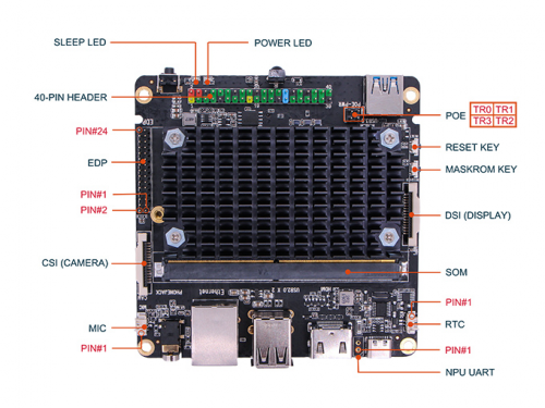
SOM
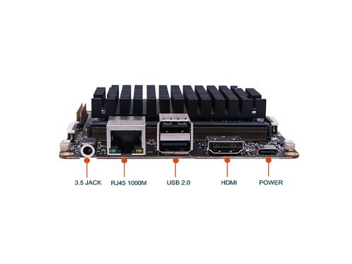
Audio: 3.5mm jack with MIC
Audio can be played through speaker or headphones using a standard 3.5mm jack with MIC.
Note that HD codec supports up to 24-bit/96KHz audio.
Buttons
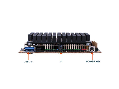
The ROCK Pi N10 board presents three buttons. They are Reset key, Maskrom key and Power key.
The Reset button serves as the hardware reset button. Short press and release the button, the system will be rebooted.
The Maskrom Button is for firmware flash/upgrade.
eDP Interface
eDP is the display interface. The definition table of the eDP connector is shown below.
As you can see, four lanes are layout.
| Pin# | Name | Pin# | Name |
|---|---|---|---|
| 1 | EDP_TX0P | 2 | EDP_TX0N |
| 3 | GND | 4 | GND |
| 5 | EDP_TX1P | 6 | EDP_TX1N |
| 7 | GND | 8 | GND |
| 9 | EDP_TX2P | 10 | EDP_TX2N |
| 11 | GND | 12 | GND |
| 13 | EDP_TX3P | 14 | EDP_TX3N |
| 15 | GND | 16 | GND |
| 17 | EDP_AUXP | 18 | EDP_AUXN |
| 19 | VDD | 20 | GND |
Ethernet
The Giga Bit Ethernet LAN with Power over Ethernet (PoE) is provided. If you are interested in POE (Power Over Ethernet), you should try it on the ROCK Pi N10 board. Additional HAT is required for powering from PoE.
HDMI
The ROCK Pi N10 is equipped with one HDMI connector and one MIPI DSI. As for HDMI, the maximum resolution is 4k@60Hz. Any HDMI monitor should work as a display for the ROCK Pi N10. As for MIPI DSI, it is designed for raw LCD pannel. HDMI and MIPI DSI can work at the same time.
The HDMI interface pin specification shows below.
| Pin# | Name |
|---|---|
| 1 | HDMI_TX2P |
| 2 | GND |
| 3 | HDMI_TX2N |
| 4 | HDMI_TX1P |
| 5 | GND |
| 6 | HDMI_TX1N |
| 7 | HDMI_TX0P |
| 8 | GND |
| 9 | HDMI_TX0N |
| 10 | HDMI_TXCP |
| 11 | GND |
| 12 | HDMI_TXCN |
| 13 | HDMI_CEC |
| 14 | NC |
| 15 | DDC_SCL |
| 16 | DDC_SDA |
| 17 | GND |
| 18 | VCC5V0_HDMI |
| 19 | PORT_HPD |
IR reveicer
IRM-3638 module is equipped. its carrier frequency is 38 KHz. And the date rate is high, up to 4000 bit/sec.
LEDs
Red LED: Power LED, also the Red LED, could be control by GPIO1_A1. The LED is ON when the GPIO1_A1 is HIGH. The LED is OFF when the GPIO is LOW.
Green Led: Reset LED.
MIPI Camera Interface
There is a wide range of camera applications in our lives. MIPI CSI 2 lane on board support 800 MP camera via FPC connector.
The MIPI CSI interface pin specification shows below.
| Pin# | Name |
|---|---|
| 1 | VCC_CAM |
| 2 | I2C4_SDA |
| 3 | I2C4_SCL |
| 4 | CAM_MCLK |
| 5 | CAM_GPIO1 |
| 6 | GND |
| 7 | MIPI_RX0_CLKP |
| 8 | MIPI_RX0_CLKN |
| 9 | GND |
| 10 | MIPI_RX0_D1P |
| 11 | MIPI_RX0_D1N |
| 12 | GND |
| 13 | MIPI_RX0_D0P |
| 14 | MIPI_RX0_D0P |
MIPI Display Interface
The ROCK Pi N10 is equipped with one HDMI connector and one MIPI DSI. As for HDMI, the maximum resolution is 4k@60Hz. Any HDMI monitor should work as a display for the ROCK Pi N10. As for MIPI DSI, it is designed for raw LCD pannel. HDMI and MIPI DSI can work at the same time.
The MIPI DSI interface pin specification shows below.
| Pin# | Name |
|---|---|
| 1 | VCC_MIPI |
| 2 | VCC_MIPI |
| 3 | GND |
| 4 | I2C_SDA_AUDIO |
| 5 | I2C_SCL_AUDIO |
| 6 | GND |
| 7 | MIPI_TX/RX_D0P |
| 8 | MIPI_TX_RX_D0N |
| 9 | GND |
| 10 | MIPI_TX/RX_CLKP |
| 11 | MIPI_TX_RX_CLKN |
| 12 | GND |
| 13 | MIPI_TX/RX_D1P |
| 14 | MIPI_TX/RX_D1N |
| 15 | GND |
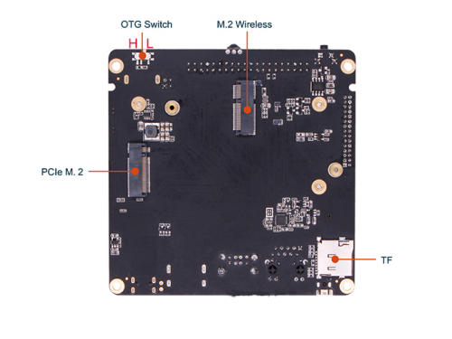
M.2 Wireless
This the M.2 Wireless Socket pin definition table.
| Name | Pin# | Pin# | Name | |
|---|---|---|---|---|
| GND | 1 | 2 | +3.3V | |
| NV | 3 | 4 | +3.3V | |
| NV | 5 | 6 | GPIO_LED | |
| GND | 7 | 8 | NC | |
| SDIO_CLK | 9 | 10 | NC | |
| SDIO_CMD | 11 | 12 | NC | |
| SDIO_D0 | 13 | 14 | NC | |
| SDIO_D1 | 15 | 16 | NC | |
| SDIO_D2 | 17 | 18 | GND | |
| SDIO_D3 | 19 | 20 | BT_HOST | |
| WIFI_HOST_WAKE | 21 | 22 | UART0_RXD | |
| WIFI_REG_ON | 23 | |||
| GND | 33 | 32 | UART0_TXD | |
| NC | 35 | 34 | UART0_CTS | |
| NC | 37 | 36 | UART0_RTS | |
| GND | 39 | 38 | NC | |
| NC | 41 | 40 | NC | |
| NC | 43 | 42 | BT_REG_NO | |
| GND | 45 | 44 | NC | |
| NC | 47 | 46 | NC | |
| NC | 49 | 48 | NC | |
| GND | 51 | 50 | RTC_CLKO | |
| NC | 53 | 52 | NC | |
| NC | 55 | 54 | NC | |
| GND | 57 | 56 | NC | |
| NC | 59 | 58 | I2C_DATA | |
| NC | 61 | 60 | I2C_CLK | |
| GND | 63 | 62 | NC | |
| NC | 65 | 64 | NC | |
| NC | 67 | 66 | NC | |
| GND | 69 | 68 | NC | |
| NC | 71 | 70 | BT_WAKE | |
| NC | 73 | 72 | 3.3V | |
| GND | 75 | 74 | 3.3V |
PCIE M.2 NGFF M-KEY SOCKET Interface
On ROCK Pi N10, M.2 connector supports up to 2T M2 NVME SSD.
The PCIE M.2 interface pin specification shows below.
| Name | Pin# | Pin# | Name | |
|---|---|---|---|---|
| GND | 1 | 2 | +3.3V | |
| GND | 3 | 4 | +3.3V | |
| PERn3 | 5 | 6 | NC | |
| PERp3 | 7 | 8 | NC | |
| GND | 9 | 10 | DAS/DSS# | |
| PETn3 | 11 | 12 | +3.3V | |
| PETp3 | 13 | 14 | +3.3V | |
| GND | 15 | 16 | +3.3V | |
| PERn2 | 17 | 18 | +3.3V | |
| PERp2 | 19 | 20 | NC | |
| GND | 21 | 22 | NC | |
| PETn2 | 23 | 24 | NC | |
| PETp2 | 25 | 26 | NC | |
| GND | 27 | 28 | NC | |
| PERn1 | 29 | 30 | NC | |
| PERp1 | 31 | 32 | NC | |
| GND | 33 | 34 | NC | |
| PETn1 | 35 | 36 | NC | |
| PETp1 | 37 | 38 | DEVSLP | |
| GND | 39 | 40 | NC | |
| PERn0/SATA-B+ | 41 | 42 | NC | |
| PERp0/SATA-B- | 43 | 44 | NC | |
| GND | 45 | 46 | NC | |
| PETn0/SATA-A- | 47 | 48 | NC | |
| PETp0/SATA-A+ | 49 | 50 | PERST# | |
| GND | 51 | 52 | CLKREQ# | |
| REFCLKN | 53 | 54 | PEWake# | |
| REFCLKP | 55 | 56 | NC | |
| GND | 57 | 58 | NC | |
| NC | 67 | 68 | SUSCLK | |
| PEDET | 69 | 70 | +3.3V | |
| GND | 71 | 72 | +3.3V | |
| GND | 73 | 74 | +3.3V | |
| GND | 75 |
PoE
PoE connector shows below.
| Name | Name |
|---|---|
| TR1 | TR0 |
| TR2 | TR3 |
Take TR0 and TR1 as the same group. And take TR2 and TR3 as another group.
Power Supply
The ROCK Pi N10 is powered by Type-C port and has a wide range of input voltage, from 9V to 21V. The ROCK Pi N10 supports USB Type-C PD 2.0 with 9V/2A, 12V/2A, 15V/2A and 20V/2A. Besides, the Pi supports QC 3.0/2.0 with 9V/2A and 12V/1.5A. The Type-C cable you using needs to support data communication. We call it USB Type-C charging data cable.
RTC
The RTC connector is designed according to the standard connector type.
| Pin# | Name |
|---|---|
| 1 | GND |
| 2 | +3.3V |
SPI Nor Flash
One SPI Nor Flash is on board. Its power supply voltage is 1.8V.
TF Card Interface
The TF card can be used as a system storage or an external storage. When it's used as a system storage, you had better choose the ones with storage space larger than 8GB. When it's used as an external storage, you can choose the ones with storage space up to 128GB. When the TF card is inserted into the TF card slot , the device will be automatically recognized by the system.
The TF card interface pin specification shows below.
| Pin# | Name |
|---|---|
| 1 | SDMMC0_D2 |
| 2 | SDMMC0_D3 |
| 3 | SDMMC0_CMD |
| 4 | VCC3V3_SYS |
| 5 | SDMMC0_CLK |
| 6 | GND |
| 7 | SDMMC0_D0 |
| 8 | SDMMC0_D1 |
| 9 | SDMMC0_DET_L |
| 10 | GND |
| 11 | GND |
| 12 | GND |
| 13 | GND |
USB
Double Type-A USB 2.0 host port
This port enables the attachment of peripherals such U Disk, keyboards, mice, USB dongle etc.
Type-A USB 3.0 port with OTG Switch
When the USB OTG Switch is switched to the host side, the Type-A USB 3.0 port also enables the attachment of peripherals such U Disk, keyboards, mice, USB dongle etc.
Compared with USB 2.0 host port, this USB 3.0 port supports On-The-Go(OTG) when the USB OTG Switch is switched to the device side. Thus the Soc is recognized as an device.
Take adb as an example. You can use a Type-A to Type-A cable as a bridge between you PC and ROCK Pi N10 Board. In addition to the system configuration, you can setup the adb tool on your PC to access ROCK Pi N10 over adb.
General purpose input-output (GPIO) connector
ROCK Pi N10 has a 40-pin expansion header. Each pin is distinguished by color.
| GPIO number | Function3 | Function2 | Function1 | Pin# | Pin# | Function1 | Function2 | Function3 | GPIO number | |
|---|---|---|---|---|---|---|---|---|---|---|
| +3.3V | 1 | 2 | +5.0V | |||||||
| 71 | I2C7_SDA | GPIO2_A7 | 3 | 4 | +5.0V | |||||
| 72 | I2C7_SCL | GPIO2_B0 | 5 | 6 | GND | |||||
| 13 | GPIO0_B5 | 7 | 8 | GPIO4_C4 | UART2_TXD | 148 | ||||
| GND | 9 | 10 | GPIO4_C3 | UART2_RXD | 147 | |||||
| 146 | PWM0 | GPIO4_C2 | 11 | 12 | GPIO0_B1 | 9 | ||||
| 150 | PWM1 | GPIO4_C6 | 13 | 14 | GND | |||||
| 149 | SPDIF_TX | GPIO4_C5 | 15 | 16 | GPIO0_B0 | 8 | ||||
| +3.3V | 17 | 18 | GPIO2_A6 | 70 | ||||||
| 40 | UART4_TXD | SPI1_TXD | GPIO1_B0 | 19 | 20 | GND | ||||
| 39 | UART4_RXD | SPI1_RXD | GPIO1_A7 | 21 | 22 | GPIO3_D4 | 124 | |||
| 41 | SPI1_CLK | GPIO1_B1 | 23 | 24 | GPIO1_B2 | SPI1_CSN0 | 42 | |||
| GND | 25 | 26 | ADC_IN1 | |||||||
| 64 | I2C2_SDA | GPIO2_A0 | 27 | 28 | GPIO2_A1 | I2C2_CLK | 65 | |||
| 74 | I2C6_SCL | GPIO2_B2 | 29 | 30 | GND | |||||
| 73 | I2C6_SDA | GPIO2_B1 | 31 | 32 | GPIO3_D5 | 125 | ||||
| 157 | GPIO4_D5 | 33 | 34 | GND | ||||||
| 68 | GPIO2_A4 | 35 | 36 | GPIO2_A2 | 66 | |||||
| 126 | GPIO3_D6 | 37 | 38 | GPIO2_A3 | 67 | |||||
| GND | 39 | 40 | GPIO1_A2 | 34 |
More details about 40-pin Header
- Pins marked with color orange are designed for debug console.
- PWM; x2, PWM0/PWM1
- SPI: x1, SPI1
- I2C: x3, I2C2/I2C6/I2C7
- UART: x2, UART3/UART4
- SPDIF_TX: x1
- ADC: x1, ADC_IN1


