Difference between revisions of "Rock/extension header"
< Rock
| Line 4: | Line 4: | ||
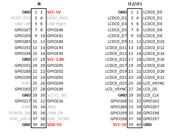
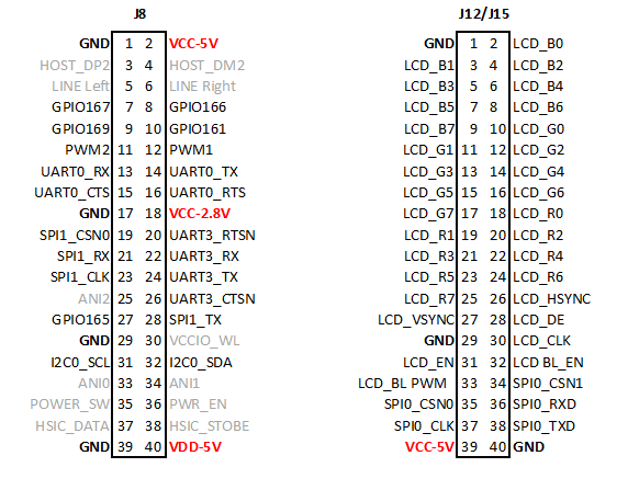
Radxa Rock has two 2.54mm 40 pins(20*2) extension header on board, which includes GPIO, I2C, SPI, Line in, USB 2.0, PWM, ADC, LCD etc interfaces. You can easily connect the breadboard or other sensor board to the rock. All the rock/rock pro/rock lite is compatible on the extension header, so it works on any hardware revision. | Radxa Rock has two 2.54mm 40 pins(20*2) extension header on board, which includes GPIO, I2C, SPI, Line in, USB 2.0, PWM, ADC, LCD etc interfaces. You can easily connect the breadboard or other sensor board to the rock. All the rock/rock pro/rock lite is compatible on the extension header, so it works on any hardware revision. | ||
| − | [[File: | + | [[File:extension_header_funca.png]] |
| + | [[File:extension_header_funcb.png]] | ||
Thanks [http://talk.radxa.com/topic/476/gpio-to-pinout-legend @zwanni] for the picture. | Thanks [http://talk.radxa.com/topic/476/gpio-to-pinout-legend @zwanni] for the picture. | ||
Revision as of 10:32, 8 October 2014
Radxa Rock has two 2.54mm 40 pins(20*2) extension header on board, which includes GPIO, I2C, SPI, Line in, USB 2.0, PWM, ADC, LCD etc interfaces. You can easily connect the breadboard or other sensor board to the rock. All the rock/rock pro/rock lite is compatible on the extension header, so it works on any hardware revision.
Thanks @zwanni for the picture.
| J8 (Near USB host and RTC battery) | |||||||
|---|---|---|---|---|---|---|---|
| USB Host | |||||||
| 1 | Ground | 2 | VCC-5V | ||||
| 3 | HOST_DP2 | 4 | HOST_DM2 | ||||
| Audio Input | |||||||
| 5 | LINE Left | 6 | LINE Right | ||||
| GPIO | |||||||
| 7 | GPIO0_A7 | 8 | GPIO0_A6 | ||||
| 9 | GPIO0_B1 | 10 | GPIO0_A1 | ||||
| PWM | |||||||
| 11 | PWM2 | GPIO3_D5 | 12 | PWM1 | GPIO3_D4 | ||
| UART0 | |||||||
| 13 | UART0_RX | GPIO1_A0 | 14 | UART0_TX | GPIO1_A1 | ||
| 15 | UART0_CTS | GPIO1_A2 | 16 | UART0_RTS | GPIO1_A3 | ||
| 17 | Ground | 18 | VCC-2.8V | ||||
| SPI1 / UART3 / GPS | |||||||
| 19 | SPI1_CSN0 | GPIO0_D7 | 20 | UART3_RTSN | GPIO1_B5 | ||
| 21 | SPI1_RX | GPIO0_D4 (GPS_PWR) | 22 | UART3_RX | GPIO1_B2 | GPS_MAG | |
| 23 | SPI1_CLK (GPS_SCLK) | GPIO0_D6 | 24 | UART3_TX | GPIO1_B3 | GPS_SIG | |
| 25 | SARADC_ANI2 (GPS_LRADC) | 26 | UART3_CTSN | GPIO1_B4 | GPS_CLK | ||
| 27 | GPIO0_A5 | 28 | SPI1_TX (GPS_MOSI) | GPIO0_D5 | |||
| I2C | |||||||
| 29 | Ground | 30 | VCCIO_WL | ||||
| 31 | I2C0_SCL | GPIO1_D1 | 32 | I2C0_SDA | GPIO1_D0 | ||
| ADC (Analog-to-digital converters) | |||||||
| 33 | SARADC_ANI0 | 34 | SARADC_ANI1 (RECOVERY) | ||||
| MISC | |||||||
| 35 | POWER_SW | 36 | PWR_EN | ||||
| 37 | HSIC_DATA | 38 | HSIC_STROBE | ||||
| 39 | Ground | 40 | VDD-5V | ||||
| J12 (Near Power Key and DC Jack) | |||||||
|---|---|---|---|---|---|---|---|
| LCD | |||||||
| 1 | Ground | 2 | LCDC0_D0 | ||||
| 3 | LCDC0_D1 | 4 | LCDC0_D2 | ||||
| 5 | LCDC0_D3 | 6 | LCDC0_D4 | ||||
| 7 | LCDC0_D5 | 8 | LCDC0_D6 | ||||
| 9 | LCDC0_D7 | 10 | LCDC0_D8 | ||||
| 11 | LCDC0_D9 | 12 | LCDC0_D10 | ||||
| 13 | LCDC0_D11 | 14 | LCDC0_D12 | ||||
| 15 | LCDC0_D13 | 16 | LCDC0_D14 | ||||
| 17 | LCDC0_D15 | 18 | LCDC0_D16 | ||||
| 19 | LCDC0_D17 | 20 | LCDC0_D18 | ||||
| 21 | LCDC0_D19 | 22 | LCDC0_D20 | ||||
| 23 | LCDC0_D21 | 24 | LCDC0_D22 | ||||
| 25 | LCDC0_D23 | 26 | LCDC0_HSYNC | ||||
| 27 | LCDC0_VSYNC | 28 | LCDC0_DE | ||||
| 29 | Ground | 30 | LCDC0_CLK | ||||
| GPIO / PWM | |||||||
| 31 | GPIO0_B0 (LCD_EN) | 32 | GPIO0_A2 (BL_EN) | ||||
| 33 | PWM3 (LCD_BL) | GPIO3_D6 | 34 | SPI0_CSN1 | GPIO1_B7 | ||
| SPI0 / UART1 | |||||||
| 35 | SPI0_CSN0 | GPIO1_A7 | UART1_RTSN | 36 | SPI0_RXD | GPIO1_A4 | UART1_RX |
| 37 | SPI0_CLK | GPIO1_A6 | UART1_CTSN | 38 | SPI0_TXD | GPIO1_A5 | UART1_TX |
| 39 | VCC-5V | 40 | Ground | ||||


